Shigeo Oshima spoke about wafer-level SSDs during the online VLSI Symposium 2020 in a presentation on the future of flash memory. The chief engineer of the NAND flash manufacturer Kioxia, formerly Toshiba Memory thus underscored the group’s claim in the development of innovative storage solutions parallel to the acquisition of the SSD division of Lite-On.
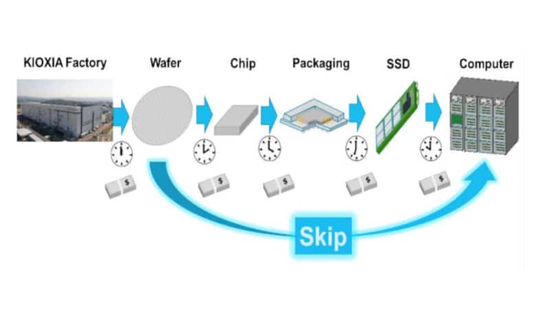
Until now, technical innovations in SSDs have been achieved primarily through additional cell layers such as 3D NAND or PLC NAND, which have further increased storage capacities. However, the manufacturing process of the various NAND types is identical. In the first step, chips are cut from a silicon wafer similar to those used in CPU and GPU production. These are then placed in a chip housing (packaging), which is then installed on the boards of SSDs and other storage media.
Higher speeds through parallel use of many chips
The new manufacturing process presented by Kioxia is intended to replace a large part of the costly production process by using the wafer itself as an SSD. The so-called “super multi-probing technology” is to be used for this purpose, which makes it possible to address the chips on the wafer directly in a computer as mass storage. At present, wafer probers are used in quality control in order to sort out faulty circuits at an early stage.
According to Kioxia, the so-called wafer-level SSDs should be significantly cheaper to manufacture due to the simplified production process and thus enable storage media with hundreds of chips, which offer significantly higher speeds due to parallel accesses than current high-end SSDs such as the recently introduced Western Digital Ultrastar DC SN840 NVMe.
The Japanese report does not contain concrete details about the technology used. However, it can be assumed that wafer-level SSDs will only be used in professional environments, for example in data centers. This is mainly due to the diameter of the wafers, which is usually 30 cm. In comparison to conventional 2.5-inch SSDs, wafer-level SSDs would therefore have to be many times larger.